SK Hynix Summer Internship
Period: 2020.07.06 ~ 2020.08.14
Department: Packgage R&D
Abstract: I worked at SK Hynix as an undergraduate student intern in 2020 summer. During the internship, I evaluated process capability of the packaging method of High Bandwidth Memory. I experimented various wafer sawing settings and evaluated them with Auto Visual Inspection and Scanning Electron Microscope. Also, I analyzed data with JMP software.
Due to the security issue of the company, it is not allowed to convey detailed information regarding my internship. Thank you for your understanding
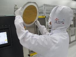
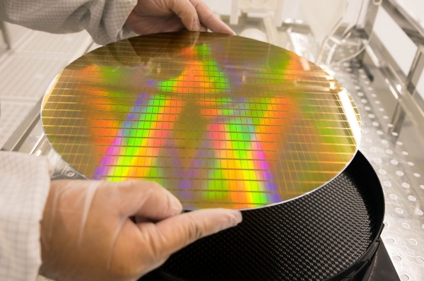
I was assigned to the DRAM packaging R&D department. Semiconductor packaging is making a black chip that we see in computers from a single wafer.
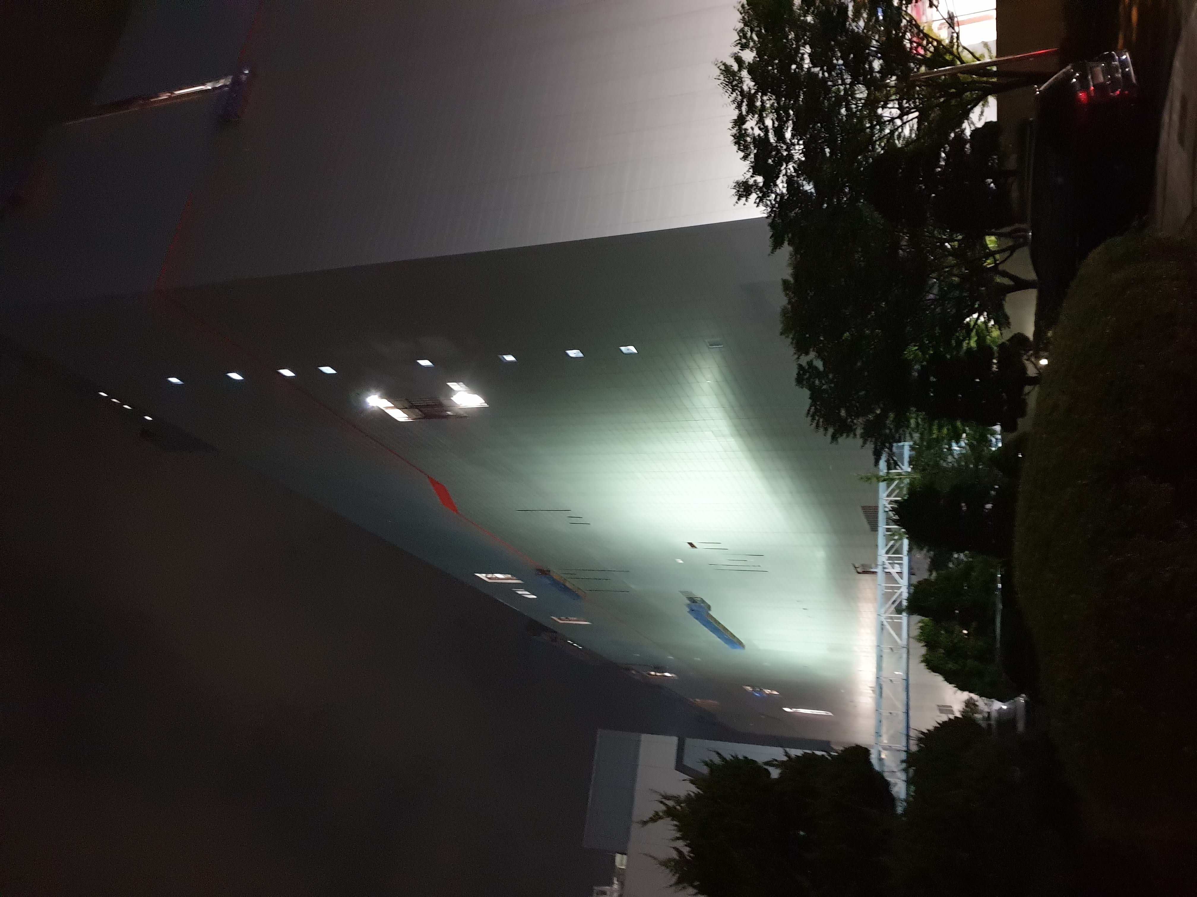
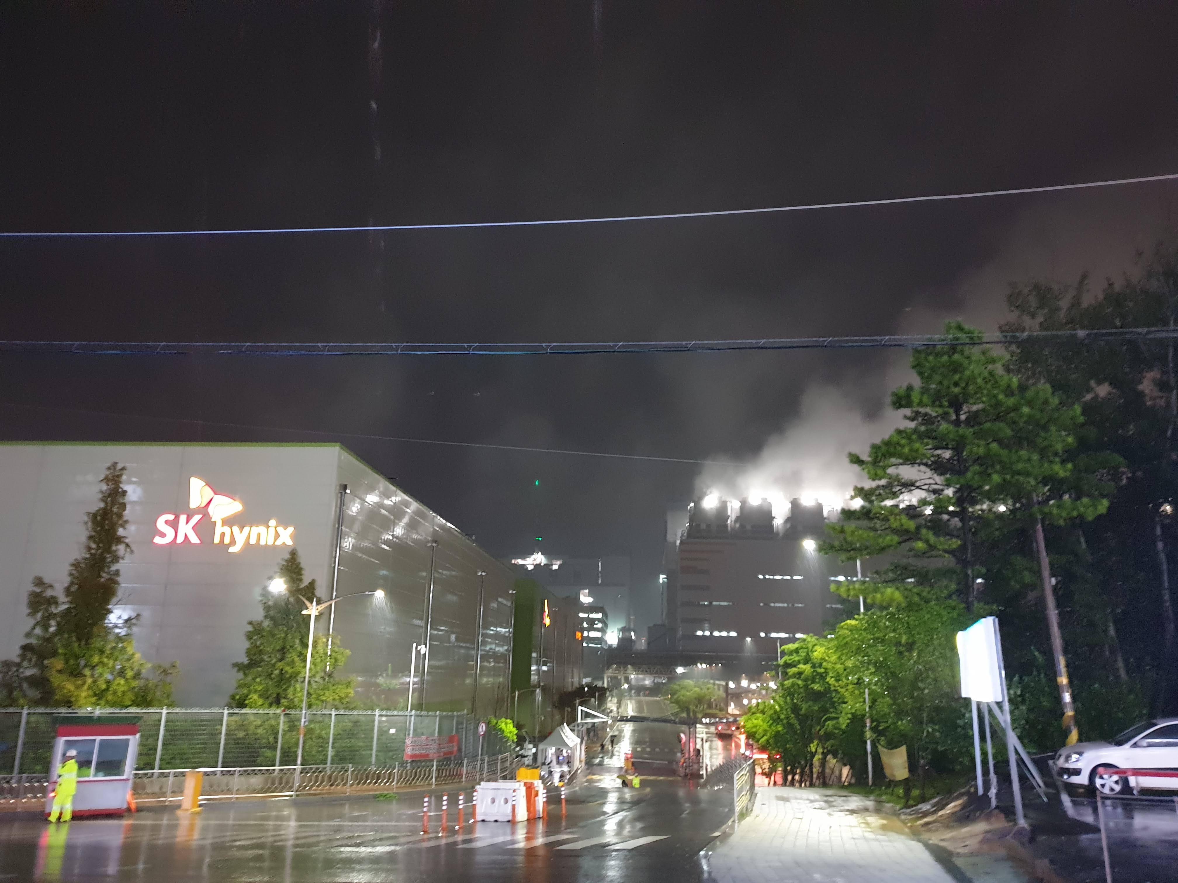
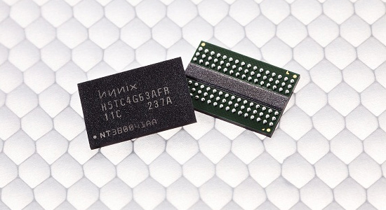 This is the start and end of Packaging process
It consists of many processes, such as wafer sawing, stacking, and molding. I participated in developing new sawing techniques for the company’s new High Bandwidth Memory. My job was a visual inspection of wafer saw with AVI (Auto Visual Inspection) and SEM (Scanning Electron Microscope). Also, I analyzed its process capability with JMP software.